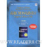
基本信息出版社:人民邮电出版社
页码:239 页
出版日期:2009年03月
ISBN:7115195986/9787115195982
条形码:9787115195982
版本:第1版
装帧:平装
开本:16
正文语种:英语
丛书名:图灵原版电子与电气工程系列
外文书名:Logical effort designing fast CMOS circuits
内容简介 《高速CMOS电路设计Logical Effirt方法(英文版)》讲述如何获得高速CMOS电路,这正是高速集成电路设计师们渴望获得的技术。在设计中,我们往往面对无数的选择,《高速CMOS电路设计Logical Effirt方法(英文版)》将告诉我们如何将这些选择变得更容易和更有技巧。《高速CMOS电路设计Logical Effirt方法(英文版)》提供了一个简单而普遍有效的方法,用于估计拓扑、电容等因素造成的延迟。
《高速CMOS电路设计Logical Effirt方法(英文版)》实用性强,适合集成电路设计师以及相关专业的师生。
作者简介 为了满足速度需求,集成电路设计师常常要痛苦地在j瞰选择中反复调整自己的设计,费时费力。两位计算机科学大师针对这一问题提出了一种简单而普遍有效的方法:LogicalEffort。本书就是他们对这一方法全面而生动的阐述。
通过本书,你不仅能够迅速地理解和掌握Logical Effort大大提高自己的工作效率,而且还能从大师著作的字里行间领悟到更多思想精髓。Ivan Sutherland著名计算机科学家。因对计算机图形学和电子设计领域的开创性贡献先后获得1988年图灵奖和1998年冯诺依曼奖。美国科学院院士、美国工程院院士和ACM会士。现任Sun公司副总裁。
Bob Sproull著名计算机科学家,美国工程院院士。现为Sun公司副总裁兼研究中心主任。Sutherlandn9长期合作者。
David Harris Harvey Mudd学院副教授。曾参与Intel安腾和奔腾II的电路设计。除本书外,他还与Weste合著了名作CMOSVLSIDesign:ACircuitsandSystemsPerspective。
目录
1 The Method of Logical Effort
1.1 Introduction
1.2 Delay in a Logic Gate
1.3 Multistage Logic Networks
1.4 Choosing the Best Number of Stages
1.5 Summary of the Method
1.6 A Look Ahead
1.7 Exercises
2 Design Examples
2.1 The AND Function of Eight Inputs
2.2 Decoder
2.3 Synchronous Arbitration
2.4 Summary
2.5 Exercises
3 Deriving the Method of Logical Effort
3.1 Model of a Logic Gate
3.2 Delay in a Logic Gate
3.3 Minimizing Delay along a Path
3.4 Choosing the Length of a Path
3.5 Using the Wrong Number of Stages
3.6 Using the Wrong Gate Size
3.7 Summary
3.8 Exercises
4 Calculating the Logical Effort of Gates
4.1 Definitions of Logical Effort
4.2 Grouping Input Signals
4.3 Calculating Logical Effort
4.4 Asymmetric Logic Gates
4.5 Catalog of Logic Gates
4.6 Estimating Parasitic Delay
4.7 Properties of Logical Effort
4.8 Exercises
5 Calibrating the Model
5.1 Calibration Technique
5.2 Designing Test Circuits
5.3 Other Characterization Methods
5.4 Calibrating Special Circuit Families
5.5 Summary
5.6 Exercises
6 Asymmetric Logic Gates
6.1 Designing Asymmetric Logic Gates
6.2 Applications of Asymmetric Logic Gates
6.3 Summary
6.4 Exercises
7 Unequal Rising and Falling Delays
7.1 Analyzing Delays
7.2 Case Analysis
7.3 Optimizing CMOS P/N Ratios
7.4 Summary
7.5 Exercises
8 Circuit Families
8.1 Pseudo-NMOS Circuits
8.2 Domino Circuits
8.3 Transmission Gates
8.4 Summary
8.5 Exercises
9 Forks of Amplifiers
9.1 The Fork Circuit Form
9.2 How Many Stages Should a Fork Use?
9.3 Summary
9.4 Exercises
10 Branches and Interconnect
10.1 Circuits That Branch at a Single Input
10.2 Branches after Logic
10.3 Circuits That Branch and Recombine
10.4 Interconnect
10.5 A Design Approach
10.6 Exercises
11 Wide Structures
11.1 An n-input AND Structure
11.2 An n-input Muller C-element
11.3 Decoders
11.4 Multiplexers
11.5 Summary
11.6 Exercises
12 Conclusions
12.1 The Theory of Logical Effort
12.2 Insights from Logical Effort
12.3 A Design Procedure
12.4 Other Approaches to Path Design
12.5 Shortcomings of Logical Effort
12.6 Parting Words
APPENDICES
A Cast of Characters
B Reference Process Parameters
C Solutions to Selected Exercises
BIBLIOGRAPHY
INDEX
……
序言 The method of logical effort is a way of thinking about delay in Mos circuits. It seeks to determine quickly a circuit's maximum possible speed and how to achieve it. It provides insight into how both the sizes of different transistors and the circuit topology itself affect circuit delay. We offer two new names for causes of delay in Mos circuits, electrical effort and logical effort. The similarity of these names reflects a remarkable symmetry between the effort required to drive an electrical load and the effort required to perform a logic function; the two forms of effort present identical and inter- changeable sources of delay. Identifying these concepts leads to a formulation that simplifies circuit analysis and allows a designer to analyze alternative circuit designs quickly.
Electrical effort is a new name for the problem overcome by electrical gain. It has long been known that the fastest driver for a large electrical load is a multistage amplifier whose gain is distributed among stages of exponentially increasing size. Thinking of what amplifiers do as compensating for electrical effort paves the way to understanding how they similarly compensate for logical effort.
文摘 To set the context of the problems addressed by logical effort, we begin by reviewing a simple integrated circuit design flow. We will see that topology selection and gate sizing are key steps of the flow. Without a systematic approach, these steps are extremely tedious and time-consuming. Logical effort offers such an approach to these problems.
Figure I. 1 shows a simplified chip design flow illustrating the logic, circuit, and physical design stages. The design starts with a specification, typically in textual form, defining the functionality and performance targets of the chip. Most chips are partitioned into more manageable blocks so that they may be divided among multiple designers and analyzed in pieces by CAD tools. Logic designers write register transfer level (RTL) descriptions of each block in a language like Verilog or VHDL and simulate these models until they are convinced the specification is correct. Based on the complexity of the RTL descriptions, the designers estimate the size of each block and create a floorplan showing relative placement of the blocks. The floorplan allows wire-length estimates and provides goals for the physical design.
Given the RTL and floorplan, circuit design may begin. There are two general styles of circuit design: custom and automatic. Custom design trades additional human labor for better performance. In a custom methodology, the circuit designer has flexibility to create cells at a transistor level or choose from a library of predefined cells. The designer must make many decisions: Should I use static CMOS, transmission gate logic, domino circuits, or other circuit families? What circuit topology best implements the functions specified in theRTL?
插图:
